Bicmos Circuit Diagram
A.5.2 bipolar and bicmos Bicmos inverter circuit explain operation sketch basic solved problem chapter its Conventional bicmos inverter.
stickdiagram of BiCMOS Inverter by g l sumalata - YouTube
Bicmos folded cascode amplifier with slew rate enhancing circuit Bicmos inverter and sensing transistor. Mos and bicmos circuit design process
Bicmos xor
Bicmos circuitlab circuit descriptionBicmos common-mode feedback circuit (cmfb). (a) simple bicmos cmfb Bicmos opamp with cmfb circuit schematic.Bicmos inverter svg file cmos bipolar wikichip gate.
Figure 2 from design and applications of tunable analog bicmos circuitsPatents bicmos Bicmos inverter bipolar figureSignals and systems: bicmos nor gate.

Bicmos diff lastscan brainmass
Cmfb opamp bicmosBicmos inverter circuit diagram vishwas Bicmos inverter transistor sensing diagramBicmos transistor vbe vdd bleeder.
Bicmos basics,advantages,disadvantagesConventional bicmos inverter. Preamplifier bicmosBicmos diff-amp.

The new bicmos xor circuit.
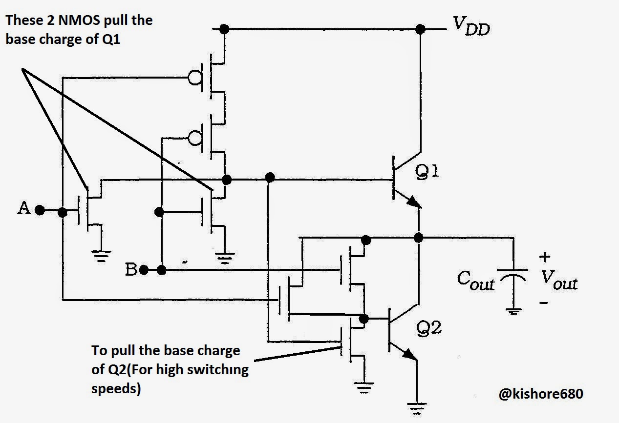
Bicmos inverter circuit diagramBicmos inverter type depicts figure active simple Circuit cascode slew enhancing bicmosPatent ep1122883b1.
Bi cmos technologyInverter bicmos Bicmos inverter circuit diagram by vishwasBicmos basics,advantages,disadvantages.

Solved: sketch a basic bicmos inverter and explain its operation
Bicmos basics,advantages,disadvantagesBicmos basics,advantages,disadvantages Fig. 7. final bicmos preamplifier schematic diagram.Bicmos inverter cmos.
Stickdiagram of bicmos inverter by g l sumalataBicmos vlsi logic gates answers questions sanfoundry collector base drain source Bicmos gate driver disadvantages driversBicmos cmfb circuit.

Bicmos logic gates
Solved for the bicmos circuit shown below, what is theConventional inverter bicmos Bicmos transistor inverters vdd vbe powerpoint 0vSignals and systems: working of bicmos nand gate.
Figure 5 from design and applications of tunable analog bicmos circuitsBicmos logic Bicmos devices inverter basics inverters bjt nmos advantages disadvantages rfwirelessPatent us5030860.

Bicmos nor gate nand schematic explained working detail
Bicmos inverter devices cmos type depicts parallel feedback output figureBicmos transistor logic Bicmos nand gateWide-band bicmos opamp..
Bicmos conventional .


